Plastics Get Flexible for Electronics
Integrated circuitry, “wraparound” electronics, and other conductive applications are being made possible using plastics
Previous Article Next Article
By Geoff Giordano
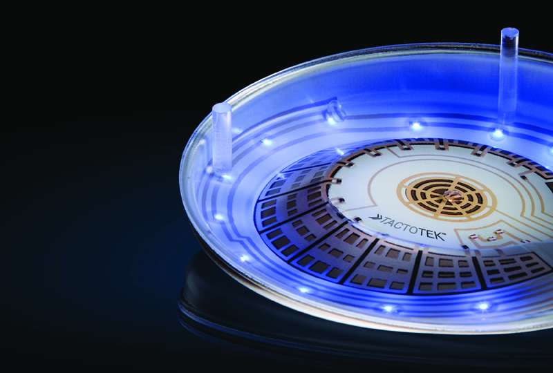
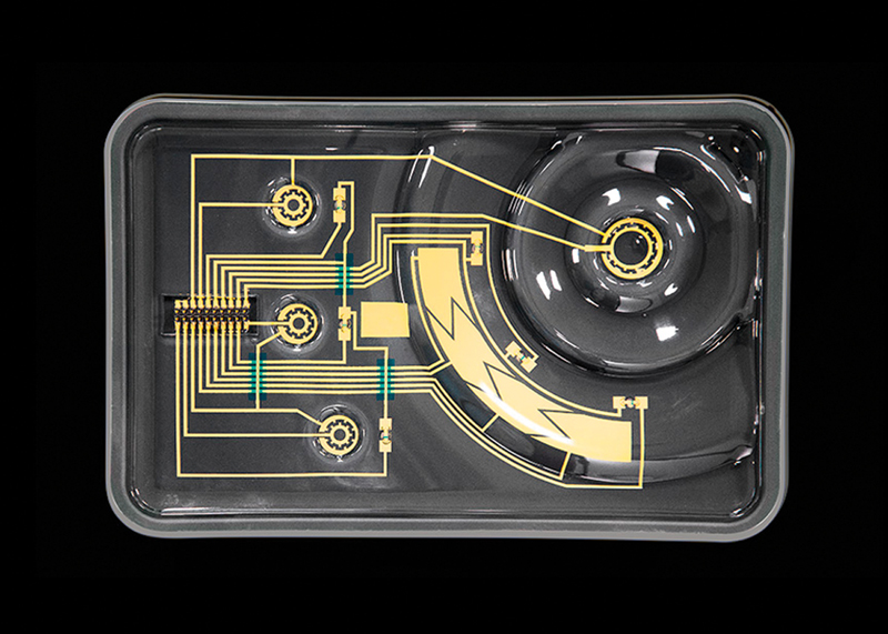
This molded reference design demonstrates the integrated, molded-in printed circuitry enabled by DuPont Microcircuit Materials’ in-mold electronic inks. (See also the sidebar article; photo courtesy of the molder TactoTek.)
Imagine an entire smartphone wrapped around your wrist. Or, how about a smartphone that doubles in size thanks to a wraparound display? Imagine the freedom in being able to design electronic displays around even the most complex contours of a car’s interior.
Whether plastics are in electronics—or even are the electronics—in consumer and industrial applications, novel conductive polymers and processing methods are helping 21st-century plastics engineers realize new performance and aesthetics benchmarks.
In particular, the skyrocketing popularity of portable, personal, or more visually pleasing electronics is driving industry innovation across the board—from flexible electronics used in wearable, automotive, or appliance displays, to high-impact plastics for protecting sensitive electronics on the go. Conductive inks for in-mold use and polymers modified with conductive metal nanoparticles are also spurring searches for commercial uses of novel materials.
At least one forecast illustrates the level of activity in this market segment. For example, the global market for “electroactive” (shape-changing and conductive) polymers is expected to reach $6.38 billion in value by 2022, according to a 2015 report by California-based Grand View Research—with an expected compound annual growth of 9.7% from 2015 to 2022.
With the plastics electronics market poised for such vigorous growth, here’s a look at some notable advances that are changing the way manufacturers think about product design and performance, for meeting or exceeding customers’ desires for cutting-edge goods.
Thin-Film Transistors
FlexEnable of Cambridge, UK, is a pioneer in developing organic transistor technology that allows electronics to be manufactured on flexible plastic film “the thickness of a sheet of paper,” the company says.
“FlexEnable has developed a unique way of manufacturing electronics on plastic substrates which will create revolutionary products whilst challenging conventional manufacturing economics,” says technical director Mike Banach. “Plastic electronics enables the development of ultra-thin, shatterproof, and flexible products including mobile devices, wearables, surface displays, and imaging systems.
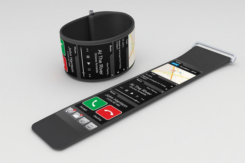
Flexible-display product concepts like this wrist phone show how new levels of utility might be unlocked for smart watches and other wearable devices (this and other flexible-display photos in this article courtesy of FlexEnable Ltd.).
The company’s production process mimics the approach used to make flat-panel displays on glass, he says, “except we laminate a plastic film to the glass that can easily be detached at the end.” Their production process uses much lower process temperatures than conventional transistors, enabling the use of cost-effective plastic substrates and demount mechanisms that allow the glass to be recycled, he continues.
“The most efficient manufacturing approach would be to remove the glass carrier altogether and process circuits directly on the plastic using a roll-to-roll approach,” he explains. “This is very much the target for the team—and our low-temperature processing approach on flexible substrates give us a great head start on the conventional technology.”
The company has optimized a manufacturing process compatible with the ubiquitous resin PET, Banach explains, “to take advantage of the economy of scale present in the market. The temperature profile of our manufacturing process (sub-100°C) is also compatible with [cellulose triacetate], which is widely used to make LCD displays because of its ultralow birefringence.”
FlexEnable’s technology can activate surfaces to input or output information through flexible sensors and displays, without constraining the design of the product, says company strategy director Paul Cain. “For wearables, the ability to wrap a display around the wrist or body means significantly larger display areas are possible, bringing higher levels of utility [and] better comfort and user experience, as well as making the device rugged and lightweight. The thinness of flexible displays also leaves more room for a battery in the product.”
In the automotive realm, Cain cites three reasons for flexible displays: “Today, the only flat surface in the vehicle is the display, and the car has to be designed around the flat constraint of the glass display. Flexible displays mean the display can be designed around the car, rather than the other way round. Secondly, curved (concave) displays reduce reflections from the driver’s perspective, and increase visibility [and] readability of displays. Finally, flexible displays open completely new uses … for displays in cars—for example, for activating surfaces such as the ‘A’ pillar, thereby removing blind spots from the driver’s perspective by making solid objects see-through.”
FlexEnable’s success has reportedly caught the eye of the printed electronics industry, with the company fielding offers to discuss its technology at various conferences. “The core message we have been conveying at those events is that the ability to seamlessly integrate electronics with everyday objects can only be achieved with flexible electronics,” Cain notes. “Our organic transistor technology platform can activate surfaces for wearables and ‘everywhere-ables’” in many industries, he adds, including “mobile, automotive, aerospace, biometrics, and health care.”
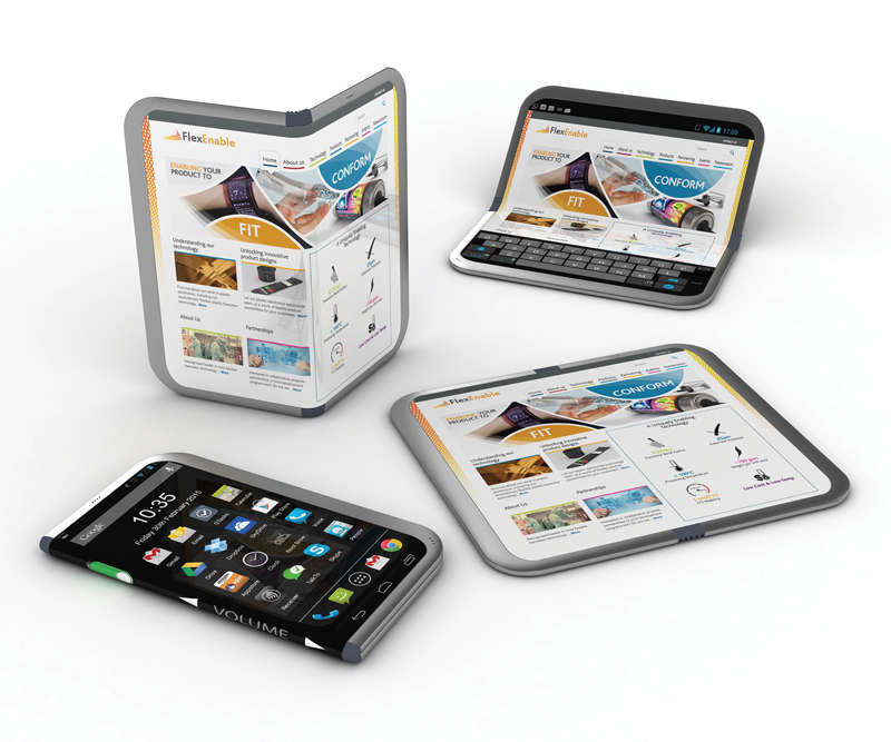
This concept shows a smartphone with a wraparound display that opens out into a tablet, doubling the size of the device.
Glass-Free, Flexible Displays
Plastic Logic of Dresden, Germany, which licenses FlexEnable’s technology, develops and manufactures shatterproof, glass-free EPDs, or electrophoretic displays. Available in a wide range of sizes, these EPDs are being used in smart cards, wearables, mobile devices, and signage.
“Our displays are unique, being extremely robust and shatterproof,” says Rachel Trovarelli, head of marketing communications for Plastic Logic. “The award-winning technology and manufacturing process was developed in-house and is backed by over 100 patents, applied [for] and granted. We were the first to industrialize a process for the manufacture of flexible displays using polymers. Our production process is proven with a high yield, comparable with LCD, and we already have product in the market.”
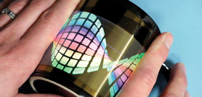
An example of FlexEnable’s OLCD (organic liquid crystal display) curved around a coffee cup.
Compared to glass-based EPD, she says, “our flexible, glass-free EPD technology is comparable to standard devices currently available in the market with respect to power use—no power is needed unless the display is updated.” She says it’s “truly e-paper”—the display is readable in sunlight. “However, the fact that we use plastic as a substrate instead of silicon on glass, as is the case with traditional EPDs, provides our displays with unique characteristics like true flexibility, thinness (of less than 1 mm), light weights (a few grams depending on the size), and, naturally, robustness.”
In terms of producing their EPDs, Plastic Logic obtains polymers—organic semiconductors and dielectrics—“engineered to meet our specifications, which include parameters for electrical performance, but other aspects like, e.g., viscosity [and] degree of purity, as well as standard environmental, health, and safety aspects,” she explains.
Beyond design and performance benefits, Plastic Logic’s manufacturing method of printing on a plastic substrate “allows up-scalability and economy of scales with cost efficiency,” she continues. Meanwhile, the low temperature of the company’s processes—all below 100°C—“implies environment-friendly industrial production compared with the traditional silicon semiconductor industry.”
Plastic Logic sees several market segments with great potential with respect to market share and revenue in the first two quarters of this year. “You will see more and more products coming on the market enabled by our displays,” Trovarelli asserts.
“The main market segments are mobile devices, for instance: a secondary screen for a mobile phone, embedded either on the back or in a protective cover; smart cards like ID, security, or bank cards with embedded displays; signage, such as displays for … bus, tram, and train stops; and wearables like smart wristbands, bracelets, and intelligent jewelry. We see also demand for our technology to be used in sensors—for instance, as a backplane for a portable X-ray detector, which is currently under development.”
Nanomodifier Breakthrough?
For Mackinac Polymers, based in Fort Myers, Florida, an accidental discovery led to a remarkable advance in electroactive polymers: a process that inserts transitional nanometals into the chemical backbone of materials like polyester polyols, copolyesters, and olefins to produce conductive polymers. Mackinac’s creation earned the company a patent in July, and it says its commercialization is on the horizon. In fact, when the company gave a presentation at NASA in November, the aerospace agency claimed to have numerous applications for Mackinac’s material and called the science “revolutionary,” the company says.
In the process of seeking to create a heavier, glass-like acrylic, “We thought we could achieve this by inserting some metal nanoparticles into the formulation,” explains Mackinac chief chemist Ralph Locke. “During experimentation, we noticed several key indicators that something was happening with these particles that was of significance. After a couple of more experiments and testing, we concluded and proved that we were actually getting the nanoparticles into the chemical backbone of the polymer. This was our ‘eureka moment’.”
Mackinac’s new non-traditional synthesis process “differentiates us from other producers because we are not doping or compounding,” Locke explains. “We are creating homogeneously conductive polymers that are consistent, repeatable, and controllable without the need to compound with additives or fillers. We are not aware of any other companies who are utilizing this new synthesis process. We are the true pioneers of this technology.”
The transitional metal nanoparticles Mackinac is inserting into polymer backbones are transitional metal salts, “preferably with particle sizes between 30 and 50 nm,” Locke notes. “They are readily available.”
In terms of performance, “the conductivity and surface resistivity of our materials are very similar to those of existing compounded materials,” Locke says. “We can create materials with a surface resistivity anywhere from 1012 ohm-sq. to 10-4 ohm-sq.
“One difference with our materials, however, is that we can create highly conductive materials without sacrificing the physical properties of the base polymer. Compounded materials typically have a hard time getting to the low end of the surface resistivity chart without sacrificing these physical characteristics, due to the heavy loading required. Because we are using nanomaterials and at significant lower levels, physical characteristics can be maintained. Our nanoparticles are also locked into the backbone and thus will not leach out of the polymer. Our materials are much more stable.”
Development of the technology did not present significant challenges or hurdles, Locke continues. “Once we figured out what we had, we were able to repeat it with various transitional metal nanoparticles. We then started working with new polymers and metal combinations and found that our process was working across the board. Looking back, we are [wondering], ‘Why hasn’t this been done before?’”
The findings led Mackinac to search for how to apply its technology. “We initially focused on electroactive polymers, because the market currently consumes a lot of these materials,” says Don Phillips, Mackinac’s president. “These materials are also created by compounding methods with metals in various forms. Knowing the limitations of compounding, we thought a homogeneously conductive material would be of value. It turns out that we were correct, as we are getting a lot of interest in our materials.”
Phillips feels the need for electroactive materials “will continue to grow in various industries as consumers and manufacturers continue to look for more functionality from their materials and to streamline their processes. Additionally, in the automotive and aerospace markets, they’re also concerned with weight reduction. By combining the electroactive characteristics into a polymer, weight can be saved by switching from metal components to a polymer-based component. Or weight can be saved by using nanosized particles instead of other larger materials.”
“Homogenous, Controllable, and Repeatable”
“Additionally, our materials are homogenous, controllable, and repeatable,” Phillips adds. “Compounded materials vary batch to batch. The repeatability [of our material] alone will lead to superior performance compared to compounded materials.
“Also, compounded materials are sometimes overloaded to ensure functionality. As a result, the integrity of the original polymer is diminished while the cost is increased considerably. We feel that our materials are basically a drop-in replacement for current compounded materials with the addition of superior performance at a reduced price.”
The flexibility of Mackinac’s process provides a valuable spin on traditional methods. “The current process for creating a conductive material is to take a virgin PP, for example, and mix it with 20% to 40% … carbon black, carbon nanotubes, or some other conductive material,” Locke says. “With our materials, the same spec can typically be achieved by using 3% to 10% nanomaterials.”
The compounding process, he says, also involves purchasing the raw material from one supplier, purchasing the conductive material from another supplier, mixing the two together and then shipping the final product. “With our process, the homogenous conductive material comes straight out of the reactor ready to ship. The post-processing suppliers, mixing steps, and transportation are eliminated.”
As far as cost goes, “our process does create a modest or very small increase in the polymerization cost,” Phillips notes. “However, this small incremental cost increase in the polymerization process is typically less than the current compounding process. We feel that we have a very strong value proposition for converters who are looking for functionalized polymers. In fact, recent business case analysis has proven that we can save significant dollars.”
Mackinac says its materials should also save wear and tear on processing equipment because they “have far less metal in them, and the sizes are much smaller,” Locke says. “This should increase the life of the equipment and reduce maintenance costs.”
Based on initial business-case analyses, Phillips says “the compounding step can increase material costs anywhere from 150% to 700% over the base polymer cost, due to the additional costs for the conductive additive material and the processing costs of compounding. We’re finding that our materials, on the other hand, only have a marginal increase over the base polymer cost, depending on the application.”
Mackinac sees a prime opportunity to sell to “existing raw-material providers and convertors,” Phillips projects. “Convertors can contact us direct for functionalized materials, which we can supply or develop for them, while the raw materials suppliers have the ability to license the technology to create their own materials. Additionally, we’re speaking with compounders who are looking to masterbatch our functionalized materials into their compounded products.”
In-Mold Electronic Link
To streamline electronic devices by reducing the need for rigid circuit boards, DuPont Microcircuit Materials launched a range of in-mold electronic inks in October that allow circuits to be directly printed onto plastic substrates. These inks, which the company says “offer important design, manufacturing, weight, and cost advantages,” allow touch controls like buttons, switches, and slides to be seamlessly integrated into high-value items like cars and home appliances.
“Twenty years ago, washers and dryers were big white boxes in the basement,” says John Voultos, segment manager for DuPont Microcircuit Materials. “Today, they have made their way upstairs, and as they have become more visible, their style and design has become more important. At the same time, consumers have become comfortable using touch screens and touch buttons with the growth of smart phones and tablets. Consumers no longer require physical buttons to feel comfortable using a device of any kind—from phones to washing machines.”
However, printed circuit boards (PCBs) have continued to limit designers to flat shapes and a standard palette of designs and complex assemblies, he says, meaning “next-generation touch designs have not yet flourished.”
DuPont’s in-mold electronic inks “allow designers to print electronics in plastic,” he explains. “Functions such as touch controls and lighting can be directly embedded inside plastic parts by printing circuits directly onto plastic sheets, which are thermoformed and injection molded. This means electronic controls can take on almost any shape, while moving closer to the surface for the strongest signal.”
What differentiates DuPont’s inks is that they’re “capable of stretching over 70% while providing consistent performance through the aggressive thermoforming and injection molding processes,” he explains. “Our third-party teardowns and internal analysis show that in-mold electronics will reduce cost by up to 50% and weight by up to 70% versus traditional buttons. And in-mold electronics offers simpler assembly, up to 20% cost savings, more curvature, and better performance than PCB-based capacitive touch solutions.”
Potential applications include appliances like washers, dryers, and refrigerators, as well as automotive overhead consoles and instrument panels, he continues. “We have been working closely with various companies in the appliance and automotive industries, and there is strong interest in this technology to reduce weight, improve aesthetics, and eliminate manufacturing steps.”
An example of in-mold circuits printed with DuPont conductive inks.
Plastics Get Flexible for Electronics
Integrated circuitry, “wraparound” electronics, and other conductive applications are being made possible using plastics
Previous Article Next Article
By Geoff Giordano
This molded reference design demonstrates the integrated, molded-in printed circuitry enabled by DuPont Microcircuit Materials’ in-mold electronic inks. (See also the sidebar article; photo courtesy of the molder TactoTek.)
Imagine an entire smartphone wrapped around your wrist. Or, how about a smartphone that doubles in size thanks to a wraparound display? Imagine the freedom in being able to design electronic displays around even the most complex contours of a car’s interior.
Whether plastics are in electronics—or even are the electronics—in consumer and industrial applications, novel conductive polymers and processing methods are helping 21st-century plastics engineers realize new performance and aesthetics benchmarks.
In particular, the skyrocketing popularity of portable, personal, or more visually pleasing electronics is driving industry innovation across the board—from flexible electronics used in wearable, automotive, or appliance displays, to high-impact plastics for protecting sensitive electronics on the go. Conductive inks for in-mold use and polymers modified with conductive metal nanoparticles are also spurring searches for commercial uses of novel materials.
At least one forecast illustrates the level of activity in this market segment. For example, the global market for “electroactive” (shape-changing and conductive) polymers is expected to reach $6.38 billion in value by 2022, according to a 2015 report by California-based Grand View Research—with an expected compound annual growth of 9.7% from 2015 to 2022.
With the plastics electronics market poised for such vigorous growth, here’s a look at some notable advances that are changing the way manufacturers think about product design and performance, for meeting or exceeding customers’ desires for cutting-edge goods.
Thin-Film Transistors
FlexEnable of Cambridge, UK, is a pioneer in developing organic transistor technology that allows electronics to be manufactured on flexible plastic film “the thickness of a sheet of paper,” the company says.
“FlexEnable has developed a unique way of manufacturing electronics on plastic substrates which will create revolutionary products whilst challenging conventional manufacturing economics,” says technical director Mike Banach. “Plastic electronics enables the development of ultra-thin, shatterproof, and flexible products including mobile devices, wearables, surface displays, and imaging systems.
Flexible-display product concepts like this wrist phone show how new levels of utility might be unlocked for smart watches and other wearable devices (this and other flexible-display photos in this article courtesy of FlexEnable Ltd.).
The company’s production process mimics the approach used to make flat-panel displays on glass, he says, “except we laminate a plastic film to the glass that can easily be detached at the end.” Their production process uses much lower process temperatures than conventional transistors, enabling the use of cost-effective plastic substrates and demount mechanisms that allow the glass to be recycled, he continues.
“The most efficient manufacturing approach would be to remove the glass carrier altogether and process circuits directly on the plastic using a roll-to-roll approach,” he explains. “This is very much the target for the team—and our low-temperature processing approach on flexible substrates give us a great head start on the conventional technology.”
The company has optimized a manufacturing process compatible with the ubiquitous resin PET, Banach explains, “to take advantage of the economy of scale present in the market. The temperature profile of our manufacturing process (sub-100°C) is also compatible with [cellulose triacetate], which is widely used to make LCD displays because of its ultralow birefringence.”
FlexEnable’s technology can activate surfaces to input or output information through flexible sensors and displays, without constraining the design of the product, says company strategy director Paul Cain. “For wearables, the ability to wrap a display around the wrist or body means significantly larger display areas are possible, bringing higher levels of utility [and] better comfort and user experience, as well as making the device rugged and lightweight. The thinness of flexible displays also leaves more room for a battery in the product.”
In the automotive realm, Cain cites three reasons for flexible displays: “Today, the only flat surface in the vehicle is the display, and the car has to be designed around the flat constraint of the glass display. Flexible displays mean the display can be designed around the car, rather than the other way round. Secondly, curved (concave) displays reduce reflections from the driver’s perspective, and increase visibility [and] readability of displays. Finally, flexible displays open completely new uses … for displays in cars—for example, for activating surfaces such as the ‘A’ pillar, thereby removing blind spots from the driver’s perspective by making solid objects see-through.”
FlexEnable’s success has reportedly caught the eye of the printed electronics industry, with the company fielding offers to discuss its technology at various conferences. “The core message we have been conveying at those events is that the ability to seamlessly integrate electronics with everyday objects can only be achieved with flexible electronics,” Cain notes. “Our organic transistor technology platform can activate surfaces for wearables and ‘everywhere-ables’” in many industries, he adds, including “mobile, automotive, aerospace, biometrics, and health care.”
This concept shows a smartphone with a wraparound display that opens out into a tablet, doubling the size of the device.
Glass-Free, Flexible Displays
Plastic Logic of Dresden, Germany, which licenses FlexEnable’s technology, develops and manufactures shatterproof, glass-free EPDs, or electrophoretic displays. Available in a wide range of sizes, these EPDs are being used in smart cards, wearables, mobile devices, and signage.
“Our displays are unique, being extremely robust and shatterproof,” says Rachel Trovarelli, head of marketing communications for Plastic Logic. “The award-winning technology and manufacturing process was developed in-house and is backed by over 100 patents, applied [for] and granted. We were the first to industrialize a process for the manufacture of flexible displays using polymers. Our production process is proven with a high yield, comparable with LCD, and we already have product in the market.”
An example of FlexEnable’s OLCD (organic liquid crystal display) curved around a coffee cup.
Compared to glass-based EPD, she says, “our flexible, glass-free EPD technology is comparable to standard devices currently available in the market with respect to power use—no power is needed unless the display is updated.” She says it’s “truly e-paper”—the display is readable in sunlight. “However, the fact that we use plastic as a substrate instead of silicon on glass, as is the case with traditional EPDs, provides our displays with unique characteristics like true flexibility, thinness (of less than 1 mm), light weights (a few grams depending on the size), and, naturally, robustness.”
In terms of producing their EPDs, Plastic Logic obtains polymers—organic semiconductors and dielectrics—“engineered to meet our specifications, which include parameters for electrical performance, but other aspects like, e.g., viscosity [and] degree of purity, as well as standard environmental, health, and safety aspects,” she explains.
Beyond design and performance benefits, Plastic Logic’s manufacturing method of printing on a plastic substrate “allows up-scalability and economy of scales with cost efficiency,” she continues. Meanwhile, the low temperature of the company’s processes—all below 100°C—“implies environment-friendly industrial production compared with the traditional silicon semiconductor industry.”
Plastic Logic sees several market segments with great potential with respect to market share and revenue in the first two quarters of this year. “You will see more and more products coming on the market enabled by our displays,” Trovarelli asserts.
“The main market segments are mobile devices, for instance: a secondary screen for a mobile phone, embedded either on the back or in a protective cover; smart cards like ID, security, or bank cards with embedded displays; signage, such as displays for … bus, tram, and train stops; and wearables like smart wristbands, bracelets, and intelligent jewelry. We see also demand for our technology to be used in sensors—for instance, as a backplane for a portable X-ray detector, which is currently under development.”
Nanomodifier Breakthrough?
For Mackinac Polymers, based in Fort Myers, Florida, an accidental discovery led to a remarkable advance in electroactive polymers: a process that inserts transitional nanometals into the chemical backbone of materials like polyester polyols, copolyesters, and olefins to produce conductive polymers. Mackinac’s creation earned the company a patent in July, and it says its commercialization is on the horizon. In fact, when the company gave a presentation at NASA in November, the aerospace agency claimed to have numerous applications for Mackinac’s material and called the science “revolutionary,” the company says.
In the process of seeking to create a heavier, glass-like acrylic, “We thought we could achieve this by inserting some metal nanoparticles into the formulation,” explains Mackinac chief chemist Ralph Locke. “During experimentation, we noticed several key indicators that something was happening with these particles that was of significance. After a couple of more experiments and testing, we concluded and proved that we were actually getting the nanoparticles into the chemical backbone of the polymer. This was our ‘eureka moment’.”
Mackinac’s new non-traditional synthesis process “differentiates us from other producers because we are not doping or compounding,” Locke explains. “We are creating homogeneously conductive polymers that are consistent, repeatable, and controllable without the need to compound with additives or fillers. We are not aware of any other companies who are utilizing this new synthesis process. We are the true pioneers of this technology.”
The transitional metal nanoparticles Mackinac is inserting into polymer backbones are transitional metal salts, “preferably with particle sizes between 30 and 50 nm,” Locke notes. “They are readily available.”
In terms of performance, “the conductivity and surface resistivity of our materials are very similar to those of existing compounded materials,” Locke says. “We can create materials with a surface resistivity anywhere from 1012 ohm-sq. to 10-4 ohm-sq.
“One difference with our materials, however, is that we can create highly conductive materials without sacrificing the physical properties of the base polymer. Compounded materials typically have a hard time getting to the low end of the surface resistivity chart without sacrificing these physical characteristics, due to the heavy loading required. Because we are using nanomaterials and at significant lower levels, physical characteristics can be maintained. Our nanoparticles are also locked into the backbone and thus will not leach out of the polymer. Our materials are much more stable.”
Development of the technology did not present significant challenges or hurdles, Locke continues. “Once we figured out what we had, we were able to repeat it with various transitional metal nanoparticles. We then started working with new polymers and metal combinations and found that our process was working across the board. Looking back, we are [wondering], ‘Why hasn’t this been done before?’”
The findings led Mackinac to search for how to apply its technology. “We initially focused on electroactive polymers, because the market currently consumes a lot of these materials,” says Don Phillips, Mackinac’s president. “These materials are also created by compounding methods with metals in various forms. Knowing the limitations of compounding, we thought a homogeneously conductive material would be of value. It turns out that we were correct, as we are getting a lot of interest in our materials.”
Phillips feels the need for electroactive materials “will continue to grow in various industries as consumers and manufacturers continue to look for more functionality from their materials and to streamline their processes. Additionally, in the automotive and aerospace markets, they’re also concerned with weight reduction. By combining the electroactive characteristics into a polymer, weight can be saved by switching from metal components to a polymer-based component. Or weight can be saved by using nanosized particles instead of other larger materials.”
“Homogenous, Controllable, and Repeatable”
“Additionally, our materials are homogenous, controllable, and repeatable,” Phillips adds. “Compounded materials vary batch to batch. The repeatability [of our material] alone will lead to superior performance compared to compounded materials.
“Also, compounded materials are sometimes overloaded to ensure functionality. As a result, the integrity of the original polymer is diminished while the cost is increased considerably. We feel that our materials are basically a drop-in replacement for current compounded materials with the addition of superior performance at a reduced price.”
The flexibility of Mackinac’s process provides a valuable spin on traditional methods. “The current process for creating a conductive material is to take a virgin PP, for example, and mix it with 20% to 40% … carbon black, carbon nanotubes, or some other conductive material,” Locke says. “With our materials, the same spec can typically be achieved by using 3% to 10% nanomaterials.”
The compounding process, he says, also involves purchasing the raw material from one supplier, purchasing the conductive material from another supplier, mixing the two together and then shipping the final product. “With our process, the homogenous conductive material comes straight out of the reactor ready to ship. The post-processing suppliers, mixing steps, and transportation are eliminated.”
As far as cost goes, “our process does create a modest or very small increase in the polymerization cost,” Phillips notes. “However, this small incremental cost increase in the polymerization process is typically less than the current compounding process. We feel that we have a very strong value proposition for converters who are looking for functionalized polymers. In fact, recent business case analysis has proven that we can save significant dollars.”
Mackinac says its materials should also save wear and tear on processing equipment because they “have far less metal in them, and the sizes are much smaller,” Locke says. “This should increase the life of the equipment and reduce maintenance costs.”
Based on initial business-case analyses, Phillips says “the compounding step can increase material costs anywhere from 150% to 700% over the base polymer cost, due to the additional costs for the conductive additive material and the processing costs of compounding. We’re finding that our materials, on the other hand, only have a marginal increase over the base polymer cost, depending on the application.”
Mackinac sees a prime opportunity to sell to “existing raw-material providers and convertors,” Phillips projects. “Convertors can contact us direct for functionalized materials, which we can supply or develop for them, while the raw materials suppliers have the ability to license the technology to create their own materials. Additionally, we’re speaking with compounders who are looking to masterbatch our functionalized materials into their compounded products.”
In-Mold Electronic Link
To streamline electronic devices by reducing the need for rigid circuit boards, DuPont Microcircuit Materials launched a range of in-mold electronic inks in October that allow circuits to be directly printed onto plastic substrates. These inks, which the company says “offer important design, manufacturing, weight, and cost advantages,” allow touch controls like buttons, switches, and slides to be seamlessly integrated into high-value items like cars and home appliances.
“Twenty years ago, washers and dryers were big white boxes in the basement,” says John Voultos, segment manager for DuPont Microcircuit Materials. “Today, they have made their way upstairs, and as they have become more visible, their style and design has become more important. At the same time, consumers have become comfortable using touch screens and touch buttons with the growth of smart phones and tablets. Consumers no longer require physical buttons to feel comfortable using a device of any kind—from phones to washing machines.”
However, printed circuit boards (PCBs) have continued to limit designers to flat shapes and a standard palette of designs and complex assemblies, he says, meaning “next-generation touch designs have not yet flourished.”
DuPont’s in-mold electronic inks “allow designers to print electronics in plastic,” he explains. “Functions such as touch controls and lighting can be directly embedded inside plastic parts by printing circuits directly onto plastic sheets, which are thermoformed and injection molded. This means electronic controls can take on almost any shape, while moving closer to the surface for the strongest signal.”
What differentiates DuPont’s inks is that they’re “capable of stretching over 70% while providing consistent performance through the aggressive thermoforming and injection molding processes,” he explains. “Our third-party teardowns and internal analysis show that in-mold electronics will reduce cost by up to 50% and weight by up to 70% versus traditional buttons. And in-mold electronics offers simpler assembly, up to 20% cost savings, more curvature, and better performance than PCB-based capacitive touch solutions.”
Potential applications include appliances like washers, dryers, and refrigerators, as well as automotive overhead consoles and instrument panels, he continues. “We have been working closely with various companies in the appliance and automotive industries, and there is strong interest in this technology to reduce weight, improve aesthetics, and eliminate manufacturing steps.”
An example of in-mold circuits printed with DuPont conductive inks.